With the development of electric vehicles, competition is becoming increasingly fierce. In addition to intelligent functions that need to meet consumers' demands, the key to advantages lies in its endurance. Extending the driving range can be achieved by reducing the overall weight of the car. Therefore, one of the goals of EV on-board charger designers is to maximize power density. SiC devices have more advantages in this regard.
Important factors in improving efficiency include device packaging and thermal performance, which play an increasingly important role in OBC design for higher power density. This article is mainly about the application potential of Infineon innovative packaging technology for future vehicle on-board chargers.
Infineon Provide Uniform Height TSC Package Devices
Shortages of through-hole device (THD) packages such as TO-247 and TO-220 are gradually emerging in a lot of applications, especially in the installation of printed circuit boards (PCBs). Surface mount devices have higher yields and reliability, and can be installed automatically. So it is increasingly replacing THD.
To help designers smoothly transit from through-hole to surface-mount technology, Infineon has developed dual-DPAK (DDPAK) and quad-DPAK (QDPAK) SiC devices. These devices feature top-side cooling (TSC) to provide similar thermal performance to through-hole devices but with the added advantage of uniform package height.
Infineon has developed DDPAK and QDPAK SMD packages for many power devices, including the CoolSiCTMG6 Schottky series and the new 750V and 1200V SiC MOSFET series in conjunction with the 650V SI SJ CoolMOSTM. The QDPAK and DDPAK SMD TSC packages with high and low voltage options have a standard height of 2.3mm. They can be used to design applications such as on-board chargers and DC-DC converters.
TSC Devices VS BSC Devices
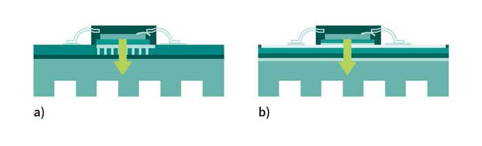
The heat dissipation methods of SMD packages include bottom-side cooling and top-side cooling. BSC-packaged devices such as D2PAK and DPAK conduct heat generated by the die downward to the bottom of the PCB board-mounted device. However, the PCB is not optimized for very high thermal conductivity, which results in a large substantial thermal barrier for the BSC device. It means that additional thermal vias are required to safely dissipate excess heat.
Source from Internet
This approach can make PCB routing more challenging because a larger area of the PCB board needs to used to place heat-dissipation electronic components. Although insulated metal substrates can improve this problem, the costs will increase.
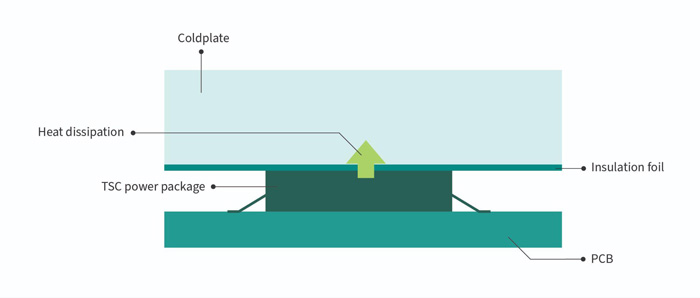
In comparison, TSC devices have more advantages. It extracts the heat generated by the die to the top of the package. The package has an exposed pad and the heat sink is connected to the pad. In this way, the thermal resistance can be reduced by 35%, and the heat dissipation path and the electrical connection on the PCB do not affect each other. This helps simplify PCB design, making it more flexible and compact, achieving higher power density and lower electromagnetic interference.
Source from Internet
Due to the improved thermal performance, there is no need for PCB board stacking or combining FR4 and IMS boards. Single FR4 is sufficient to accommodate all components and requires only a small number of connectors. This helps reduce BOM, thereby reducing overall system cost.
In addition, TSC technology can also provide optimized power loop design, thereby improving reliability. The driver can be placed close to the power switch, and its low stray inductance also reduces the effects of loop parasitics, resulting in less ringing on the gate, higher performance, and lower risk of failure.
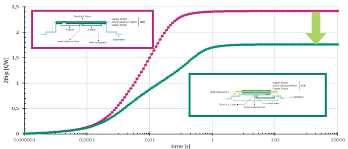
Infineon proposes an innovative DCB-on-package way to implement TSC, in which the semiconductor die remains directly connected to the lead frame.
This approach provides additional cooling capacity. Second, connecting the DCB on the package eliminates the flexibility of chip interconnection and redistribution. In addition, since conventional welding is no longer used, using diffusion welding for die connection enables the thickness of the die connection material to be significantly reduced from approximately 50 μm to only 1.2 μm.
Benefits of Diffusion Welding
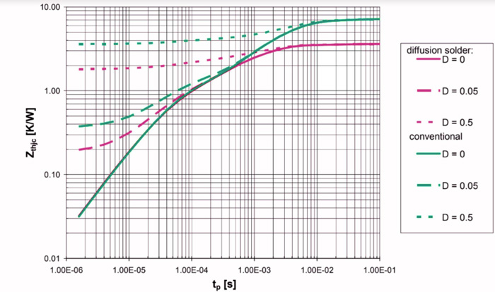
SiC has very high performance, but the die is typically small, only a few mm2, and attaching it to the package with traditional solder requires good process control. The surface energy of the solder drop can cause the die to tilt, an effect that can subsequently hinder the wire bonding process.
Diffusion solder has excellent material properties and smaller bonding wire thickness. Reducing the amount of solder in the device can significantly improve thermal conductivity. Since the solder does not melt until it comes into contact with the substrate, this can be avoided by using diffusion soldering. It also allows the assembly of multiple dies on a single leadframe because subsequent heating steps do not affect the initial die placement accuracy. In addition, since the solder does not remelt, there is no die deflection caused by surface tension.
Source from Internet
It can be seen from the measurement results that the thermal resistance of the Schottky diode junction and package lead frame quality inspection is reduced by approximately 40% compared to using conventional solder. This significant improvement in thermal performance means that for a given chip area, the maximum quiescent current rating can be increased, allowing for higher maximum power.
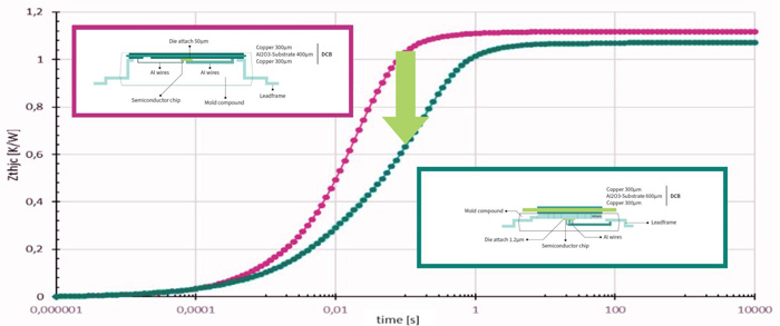
Source from Infineon
Infineon conducted theoretical simulations on SiC die sizes of 4 mm2 and 14 mm2 to compare the thermal performance of in-package DCB and on-package DCB methods as a function of applied current pulses. The results show that the on-package DCB provides better thermal performance, allowing it to withstand higher currents.
Conclusion
Device packaging and cooling mechanisms are increasingly important to maximize power density. Infineon provides devices with a unified height. In addition to meeting the requirements of current OBC designers, Infineon has also been looking to the future to seek new solutions to further improve TSC, as it can achieve more compact, more flexible devices with higher thermal performance.